Today’s coating processes provide the capability to produce anti-reflective (AR) coatings, bandpass filters, separation filters, high laser damage threshold coatings, mirror coatings, etc. with high precision and high yields. The production environment is based on batch-coating processes and component sizes that range from mm to meter. Generally, one function such as limited wavelength coverage is provided by the standard coating process.
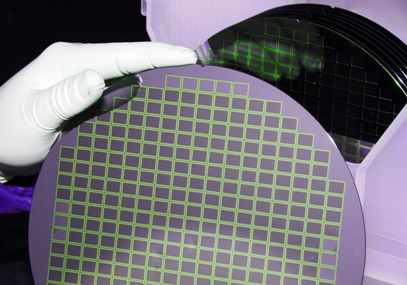
The desire to incorporate optical coatings at the wafer-level stage was inspired by semiconductor manufacturing practices, and has led to an evolution in specialty optics requirements. Development of processes that would enable complex multi-layer coatings to be incorporated into wafer manufacture called for new thinking. It allowed for the reduction of deposition temperatures and incorporation of photolithographic steps to define smaller coated areas.
An example of the use of wafer-level integration and production is the manufacture of solar cells. The most efficient solar arrays in production are composed of multi-junction thin film PV cells such as: Cu (In,Ga) Se2 (CIGS), CuInSe2 (CIS), CuInSSe (CISS), and the GaAs-based compositions InGaP/InGaAs/Ge triple junction cells developed for space applications. The latter cells power orbiting missions for NASA, NOAA, DoD and for commercial applications in communication, entertainment and GPS satellites. The junction and absorber layers, buffer interlayers, contact electrodes, and AR coatings are all deposited at the wafer stage. Advances now allow for solar cell wafer diameters to be 150 mm.

The promise of high density, high speed communications and data networks inspired the development of DWDM (dense wavelength division multiplexing) filter deposition and subsequent mm-sized dicing, with associated mounting and testing techniques. Currently, the proliferation of miniaturized spectral analytical instrumentation requirements and their expanding applications have inspired the introduction of wafer-level manufacturing processes for band-pass filters. This satisfies the needs of low-cost miniature non-scanning spectrometer applications.
Advances in Coating Technology Set the Stage for Miniaturized Optics Production
In the case of DWDM filters, where spectral bandwidths can be as narrow as 0.4 nm (0.02% relative to the center wavelengths near 1550 nm), the state of coating technology had to be quickly advanced over the existing pace of development in the 1990s [1]. As indicated by the name, many narrow spectral bands separated by small intervals are multiplexed and transmitted down a single fiber, then de-multiplexed at the receiver end – thus dramatically increasing the data capacity of a single optical fiber. This optics network is the backbone of Internet and other high data rate applications. Revolutionary improvements in: deposition process accuracy, precision, temporal stability and coating material consistency were necessary to make DWDM filters fulfill their promise. A greater understanding of the factors that influence coating performance at the nano-meter level was derived as a result.