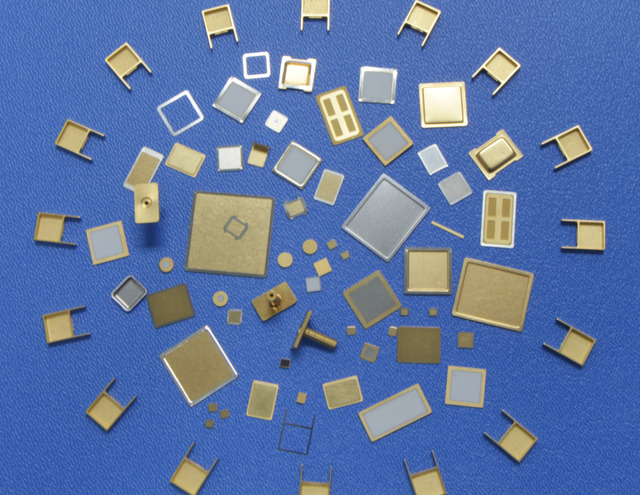


CERAMIC PACKAGES WITH HIGH RELIABILITY
Materion manufactures a line of ceramic packages for RF and microwave transistors. We can also fabricate new designs to meet customer requirements for microelectronic packaging.
Packages are available in surface mount designs and bolt-down versions. Our high-quality ceramic packages support a wide variety of RF power transistors and MMICs (monolithic microwave integrated circuit). That includes transistors fabricated in Si, GaAs and GaN. We can incorporate flanges of advanced materials to meet high-power density requirements in RF power transistors (and more).
INDUSTRY STANDARD FOR SI AND GAN RF POWER TRANSISTORS
Our ceramic air cavity packages deliver consistently high performance for transmission in the 500 MHz to 3.5 GHz frequency range. Brazed construction provides excellent mechanical reliability for use in microelectronic packaging designs that meet rigorous performance standards.
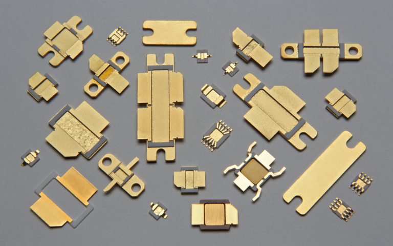
PATENTED CUPACK PACKAGES FOR ULTIMATE PERFORMANCE
Our unique ceramic packages are electrolytically plated with gold and nickel. They're compatible with a wide range of die attach materials. Our high-quality CuPack™ packages meet specific standards for low thermal resistance and low RF loss. Consult the CuPack data sheet, or connect with our engineering team for technical details including cavity area measurements, material construction, bonding and footprint design.
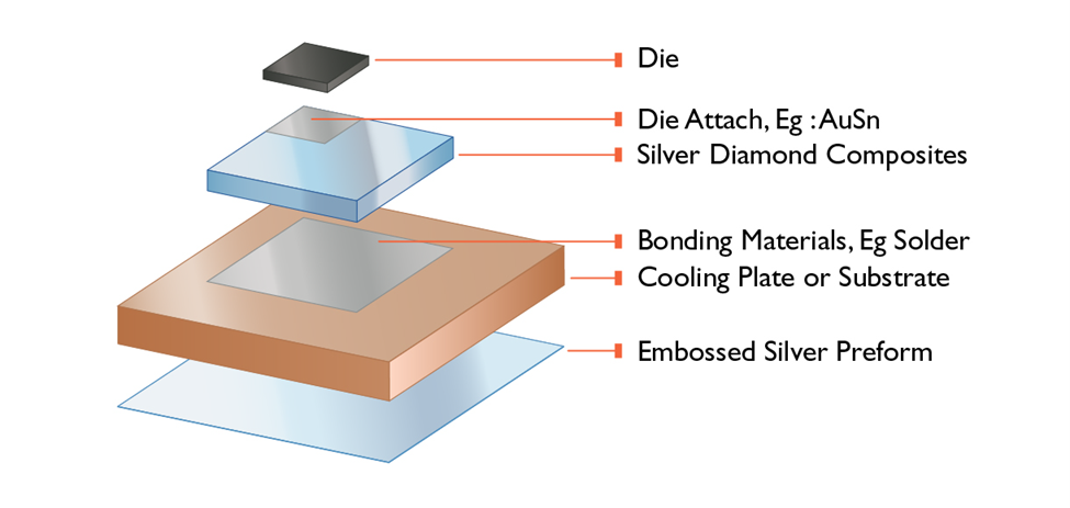
THERMAL DISSIPATION OF SILVER AND GOLD THIN FOILS WITH YOUR BRANDING
Materion also manufactures high-purity elements in alloys such as silver and gold-based alloy preforms. These preforms are used in a range of industries that require superior joining in sensitive electrical assemblies, i.e., high-power semiconductor devices, microelectronics packaging for hermetic applications, military and defense, RF and microwave devices and communications.
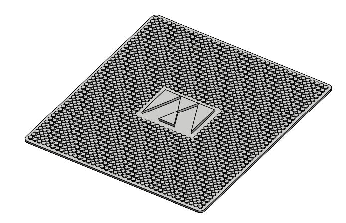
Embossed silver preforms offer precise contact between thermal spreaders and flanges. Materion's latest GenPack™ RF packaging encompasses effective thermal transfer flanges such as silver diamond, CPC and CMC, and can feature your logo/brand.
THERMAL CONTACT MATERIALS TO SUPPORT GENPACK RF PACKAGES
Materion has a robust offering of embossed metal alloy preforms that includes:
- High purity of 99.995% in silver and gold material
- Tack welding on the preform to substrates
- Embossing on top and bottom surfaces for better surface contact
- Holes and relief on the preform design to match mounting to thermal spreading flanges
- Soft tool for smaller volume and hard tool for high-volume production, resulting in shorter lead times
- Waffle, tape, or reel-based packaging
- Silver material with a thermal conductivity of 430 w/m K (ideal when applied between thermal spreaders/flanges and substrates)
Benefits
- Custom designs available
- Choice of materials and sizes
- Low thermal resistance and low RF loss
- Compatible with high-power devices
- Excellent mechanical reliability
Applications
- Aerospace
- High-power semiconductor devices
- Military / defense systems
- RF and microwave devices
- Communications
- Base stations
- Wireless