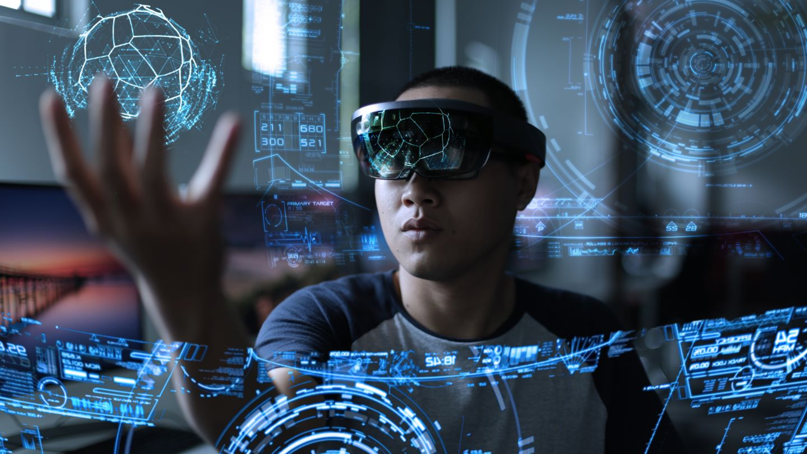
Materion delivers next-generation optics solutions that enable virtual/augmented reality, sensing technologies that make autonomous driving possible, and optical technology that enables adaptive cruise control, head-up displays, and intelligent headlights to name a few.
Materion is a globally recognized leader in customized optical thin-film coatings and components for the photonics industry. Our Precision Optics business delivers optical thin-film coatings that enable advances in automotive, consumer, defense, industry, life science, semiconductors and space products. We provide the world’s most extensive offering of precision optical components, optical thin-film coatings, and optical assemblies.
We also provide the comprehensive engineering expertise using innovative process technologies ranging from custom manufacture and supply to a broad array of products from UV through Far IR. Many of our individual product lines serve diverse markets and enable a number of different technologies and applications.
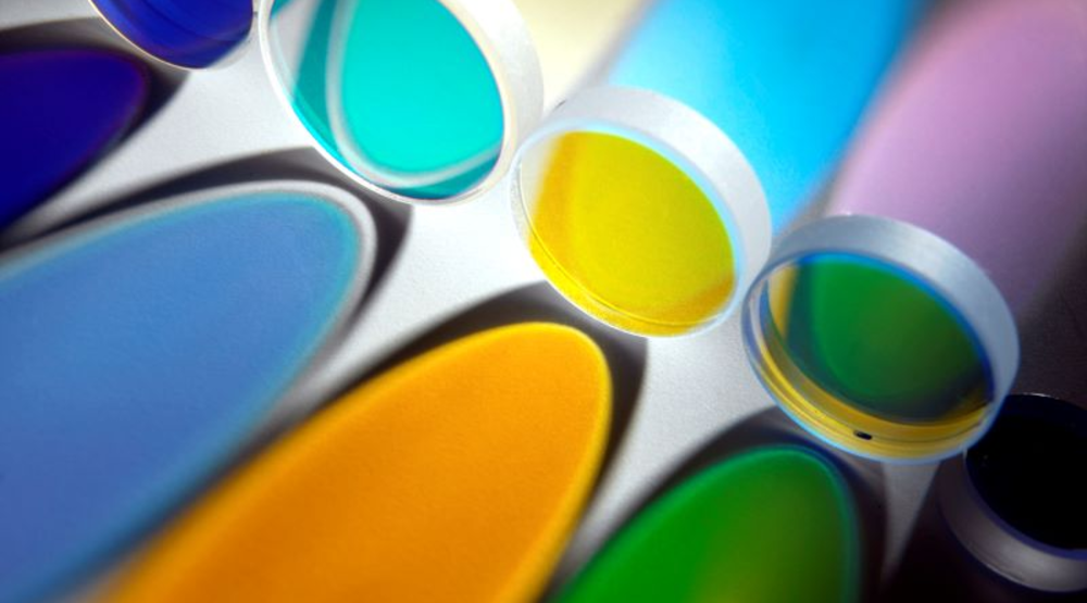
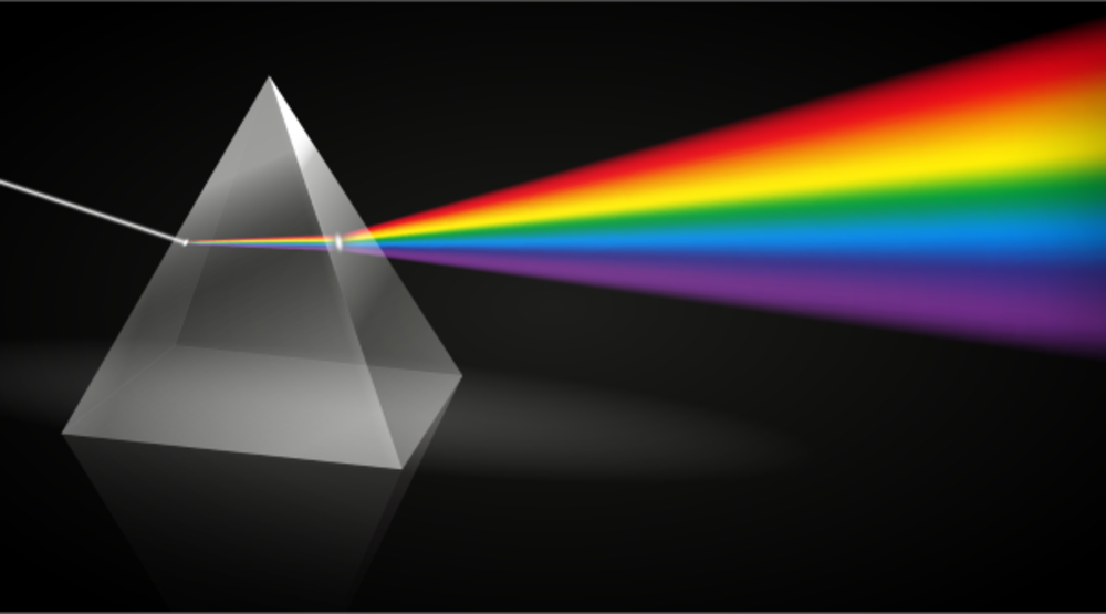
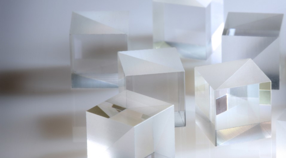
Cutting edge optical components that manage the spectrum of light through processes like high-precision filtering, reflecting, focusing and polarizing.
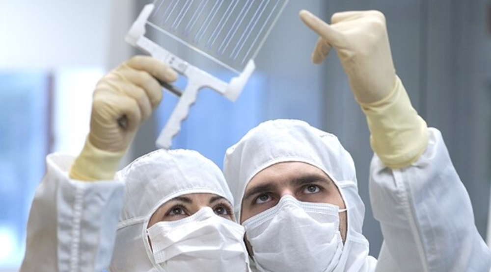
Manufacturing high-quality optical coatings requires sophisticated process technology combined with in-depth process know-how.
We collaborate with our customers and partners to make optical subassemblies easy for them in system-level applications.
Our CoatingPlus technology delivers additional process steps to maximize functionality and performance in certain applications.
In addition to our own engineers, our partnerships with scientific institutes and leading universities uniquely position us to partner with customers to develop ideas when they are still only ideas.